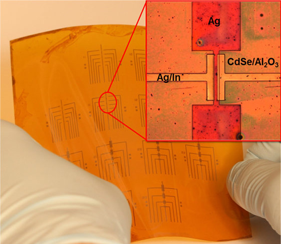
University of Pennsylvania engineers have developed a simplified new approach for making transistors by sequentially depositing their components in the form of liquid nanocrystal “inks.” The new process open the door for transistors and other electronic components to be built into flexible or wearable applications. It also avoids the highly complex current process for creating transistors, which requires high-temperature, high-vacuum equipment. Also, the new lower-temperature process is compatible with a wide array of materials and can be applied to larger areas.
First transistors made entirely of nanocrystal ‘inks’ in simplified process


